
Contact : Françoise PILLIER +331 44 27 42 01
Equipment:
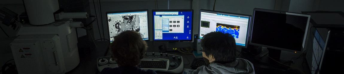
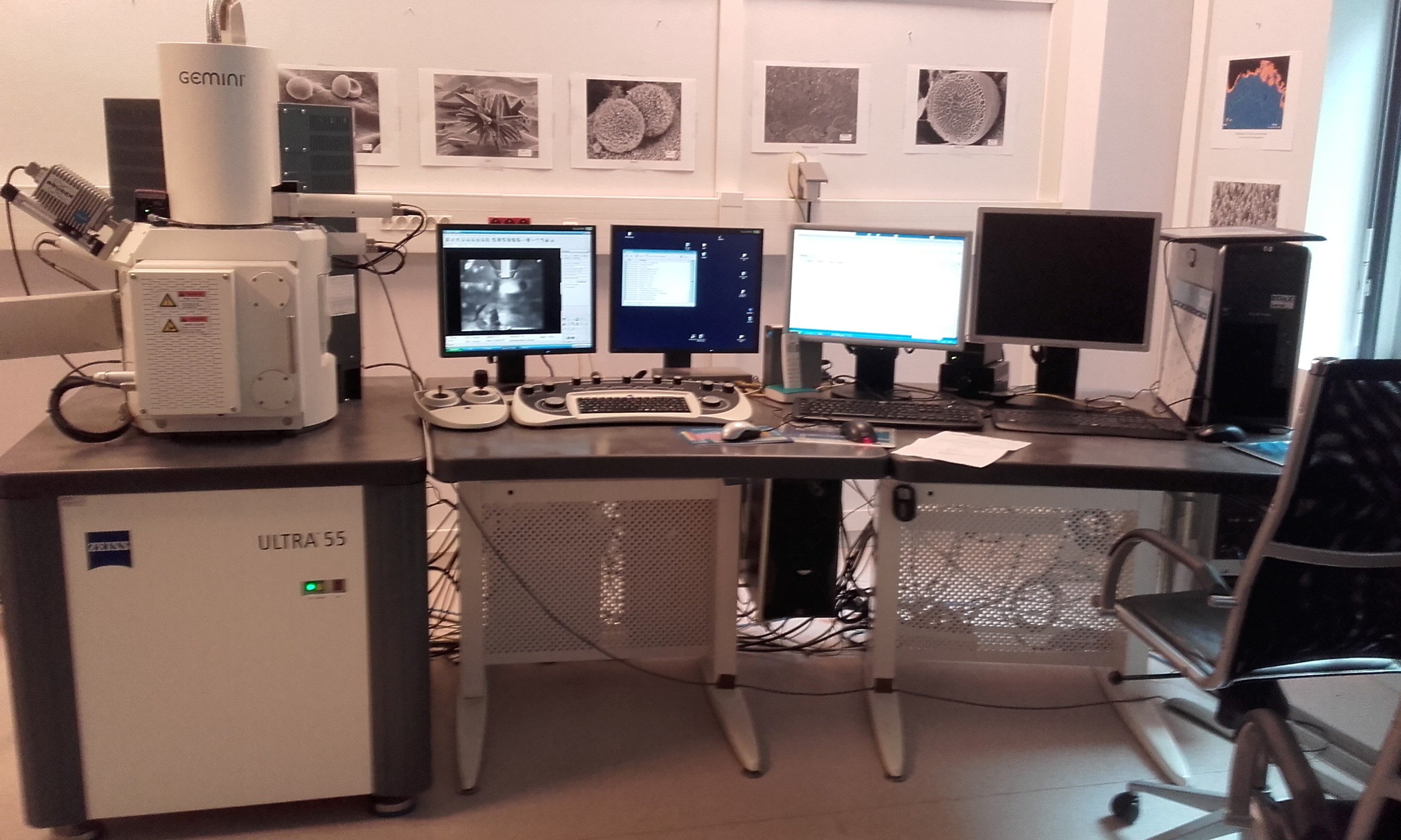
Scanning electron microscope with field emission gun (SEM-FEG) ULTRA 55 ZEISS equipped with energy-dispersive X-ray spectroscopy EDX Bruker QUANTAX and also with a electron backscatter diffraction EBSD
 Secondary electron (SE2, InLens)
- Backscattered electron (AsB, EsB)
- X-ray microanalysis (EDS)
- EBSD
- sputtering (Cressington 108)
- Carbon coating (Cressington 208)
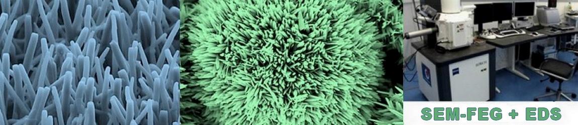
Secondary electron imaging
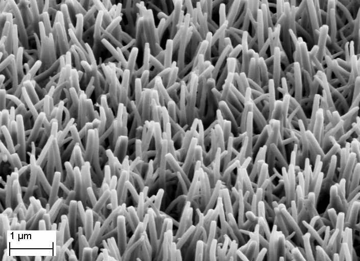 Observation of sample topography with a secondary electron detector down to nanoscale.
Electrochemically synthesized polypyrrole nanowires
(Electrochem. Commun. 2009, 11, 298).
Backscattered electron imaging
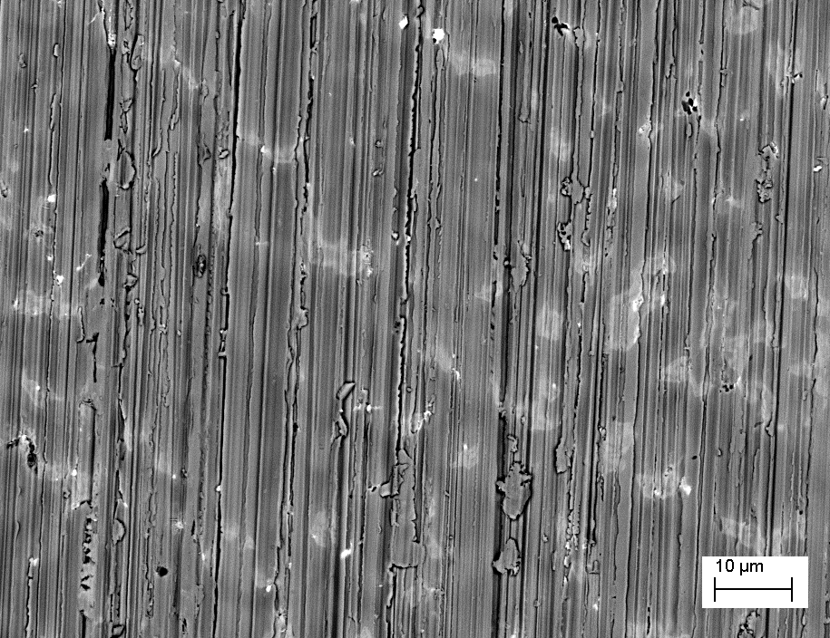
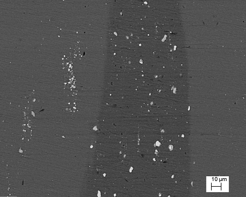 Observation of the different phases of a sample depending on their atomic number detecting of backscattered electrons
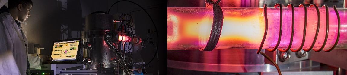
Welding between two aluminium alloys
(2024 et 7475immersed in a 0.1M Na2SO4 solution)
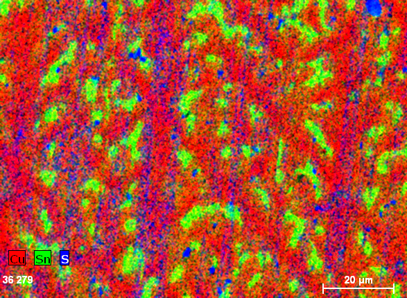
Elementary analysis
Qualitative and quantitative analysis (with standards) of the elements in the material and mapping
Spectrum
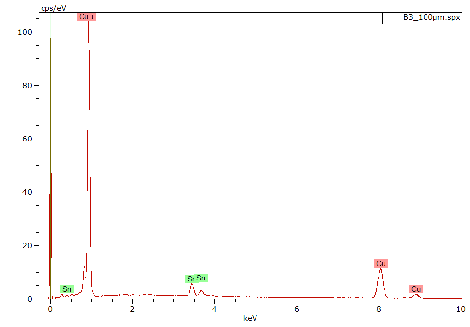
Cu 90.10%
Sn 9.90%
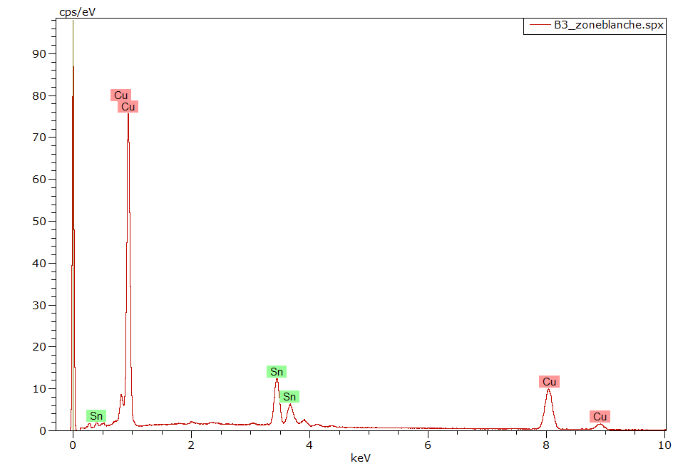
Cu 75.17 %
Sn 24.83%
Mapping
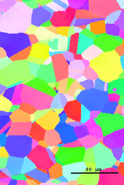
EBSD
Characterization of the crystallographic properties of sample